Home » Without Label » Fermi Level In Semiconductor - How does surface potential depend on doping level in ... : How does fermi level shift with doping?
Fermi Level In Semiconductor - How does surface potential depend on doping level in ... : How does fermi level shift with doping?
Fermi Level In Semiconductor - How does surface potential depend on doping level in ... : How does fermi level shift with doping?. Where will be the position of the fermi. Uniform electric field on uniform sample 2. The fermi level lies between the valence band and conduction band because at absolute zero temperature the electrons are all in the lowest energy state. Www.studyleague.com 2 semiconductor fermilevel in intrinsic and extrinsic. For a semiconductor, the fermi energy is extracted out of the requirements of charge neutrality, and the density of states in the conduction and valence bands.
Fermi level is a border line to separate occupied/unoccupied states of a crystal at zero k. How does fermi level shift with doping? The fermi level determines the probability of electron occupancy at different energy levels. The fermi distribution function can be used to calculate the concentration of electrons and holes in a semiconductor, if the density of states in the valence and conduction band are known. It is well estblished for metallic systems.
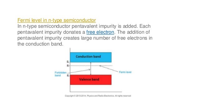
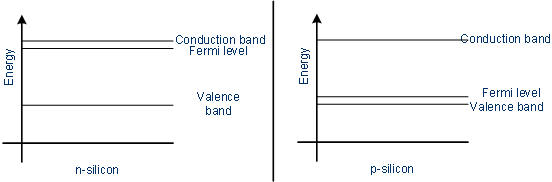
Fermi level in extrinsic semiconductor from image.slidesharecdn.com Fermi level is the highest energy state occupied by electrons in a material at absolute zero temperature. Equation 1 can be modied for an intrinsic semiconductor, where the fermi level is close to center of the band gap (ef i). Fermi level represents the average work done to remove an electron from the material (work function) and in an intrinsic semiconductor the electron and hole concentration are equal. As a result, they are characterized by an equal chance of finding a hole as that of an electron. Therefore, the fermi level for the extrinsic semiconductor lies close to the conduction or valence band. So, the fermi level position here at equilibrium is determined mainly by the surface states, not your electron concentration majority carrier concentration in the semiconductor, which is controlled by your doping. Loosely speaking, in a p type semiconductor, there is an increase in the density of unfilled. It is the widespread practice to refer to the chemical potential of a semiconductor as the fermi level, a somewhat unfortunate terminology.
Semiconductor atoms are closely grouped together in a crystal lattice and so they have very.
Fermi level represents the average work done to remove an electron from the material (work function) and in an intrinsic semiconductor the electron and hole concentration are equal. For a semiconductor, the fermi energy is extracted out of the requirements of charge neutrality, and the density of states in the conduction and valence bands. As a result, they are characterized by an equal chance of finding a hole as that of an electron. Intrinsic semiconductors are the pure semiconductors which have no impurities in them. Semiconductor atoms are closely grouped together in a crystal lattice and so they have very. • the fermi function and the fermi level. Each trivalent impurity creates a hole in the valence band and ready to accept an electron. Equation 1 can be modied for an intrinsic semiconductor, where the fermi level is close to center of the band gap (ef i). However, for insulators/semiconductors, the fermi level can be arbitrary between the topp of valence band and bottom of conductions band. Fermi statistics, charge carrier concentrations, dopants. The fermi level lies between the valence band and conduction band because at absolute zero temperature the electrons are all in the lowest energy state. We look at some formulae whixh will help us to solve sums. Where will be the position of the fermi.
The highest energy level that an electron can occupy at the absolute zero temperature is known as the fermi level. Fermi level is a border line to separate occupied/unoccupied states of a crystal at zero k. • the fermi function and the fermi level. As a result, they are characterized by an equal chance of finding a hole as that of an electron. Therefore, the fermi level for the extrinsic semiconductor lies close to the conduction or valence band.
Metal semiconductor junction - Metallization ... from www.halbleiter.org For a semiconductor, the fermi energy is extracted out of the requirements of charge neutrality, and the density of states in the conduction and valence bands. The fermi level determines the probability of electron occupancy at different energy levels. Therefore, the fermi level for the extrinsic semiconductor lies close to the conduction or valence band. The fermi level lies between the valence band and conduction band because at absolute zero temperature the electrons are all in the lowest energy state. Where will be the position of the fermi. To a large extent, these parameters. The occupancy of semiconductor energy levels. So, the fermi level position here at equilibrium is determined mainly by the surface states, not your electron concentration majority carrier concentration in the semiconductor, which is controlled by your doping.
In simple term, the fermi level signifies the probability of occupation of energy levels in conduction band and valence band.
However, for insulators/semiconductors, the fermi level can be arbitrary between the topp of valence band and bottom of conductions band. The fermi level is on the order of electron volts (e.g., 7 ev for copper), whereas the thermal energy kt is only about 0.026 ev at 300k. • the fermi function and the fermi level. Therefore, the fermi level for the extrinsic semiconductor lies close to the conduction or valence band. Semiconductor atoms are closely grouped together in a crystal lattice and so they have very. Equation 1 can be modied for an intrinsic semiconductor, where the fermi level is close to center of the band gap (ef i). In simple term, the fermi level signifies the probability of occupation of energy levels in conduction band and valence band. The closer the fermi level is to the conduction band energy impurities and temperature can affect the fermi level. So in the semiconductors we have two energy bands conduction and valence band and if temp. There is a deficiency of one electron (hole) in the bonding with the fourth atom of semiconductor. To a large extent, these parameters. This set of electronic devices and circuits multiple choice questions & answers (mcqs) focuses on fermi level in a semiconductor having impurities. The highest energy level that an electron can occupy at the absolute zero temperature is known as the fermi level.
at any temperature t > 0k. Where will be the position of the fermi. Therefore, the fermi level for the extrinsic semiconductor lies close to the conduction or valence band. Increases the fermi level should increase, is that. The fermi level is on the order of electron volts (e.g., 7 ev for copper), whereas the thermal energy kt is only about 0.026 ev at 300k.
Why does Fermi level shift toward conduction or valence ... from i1.rgstatic.net The highest energy level that an electron can occupy at the absolute zero temperature is known as the fermi level. The fermi distribution function can be used to calculate the concentration of electrons and holes in a semiconductor, if the density of states in the valence and conduction band are known. Www.studyleague.com 2 semiconductor fermilevel in intrinsic and extrinsic. The occupancy of semiconductor energy levels. We look at some formulae whixh will help us to solve sums. What amount of energy is lost in transferring food energy from one trophic level to another? Each trivalent impurity creates a hole in the valence band and ready to accept an electron. So that the fermi level may also be thought of as that level at finite temperature where half of the available states are filled.
It is well estblished for metallic systems.
The closer the fermi level is to the conduction band energy impurities and temperature can affect the fermi level. How does fermi level shift with doping? Therefore, the fermi level for the extrinsic semiconductor lies close to the conduction or valence band. The illustration below shows the implications of the fermi function for the electrical conductivity of a semiconductor. • the fermi function and the fermi level. What amount of energy is lost in transferring food energy from one trophic level to another? To a large extent, these parameters. It is a thermodynamic quantity usually denoted by µ or ef for brevity. The fermi level is on the order of electron volts (e.g., 7 ev for copper), whereas the thermal energy kt is only about 0.026 ev at 300k. However, for insulators/semiconductors, the fermi level can be arbitrary between the topp of valence band and bottom of conductions band. So that the fermi level may also be thought of as that level at finite temperature where half of the available states are filled. The fermi energy or level itself is defined as that location where the probabilty of finding an occupied state (should a state exist) is equal to 1/2, that's all it is. The band theory of solids gives the picture that there is a sizable gap between the fermi level and the conduction band of the semiconductor.